3D-Mintegration
Challenge
Dr Harald Egnar of the Fraunhofer Institute
stated that “the groundbreaking work
carried out in the FAMBOS project had led
to securing European funding to further develop
the technology and that significant industrial
interest was being shown in the technology. |
This project is destined to revolutionise the way
small, complex products and components are manufactured
by providing a radical, new way of thinking for
the end-to-end design, processing, assembly, packaging,
integration and testing of complete 3D miniaturised/
integrated (“3D Mintegrated”) products.
The work of this Grand Challenge will form the basis
for next generation automotive, aerospace, telecommunications,
medical and consumer products that will combine
significantly improved performance with higher added
value, sustainability and eco-efficiency. The 3D-Mintegration
project will also give companies valuable insight
into how evolving practices in this field worldwide
may be adopted and adapted for optimal exploitation
in the UK. Over twenty companies have shown an interest
in the technology including: BAE Systems, Unilever,
AstraZenica and GlaxoSmithKline.
Current micro engineering techniques are based upon
those used for semiconductors, and so tend to permit
only the manufacture of products based on single
materials, typically in planar configurations. There
is a need to address the restrictive issues of materials
and very high capital costs by developing entirely
new design and manufacturing techniques underpinned
by modelling, simulation and risk mitigation procedures
to ensure that these new manufacturing techniques
can be exploited by industry with confidence.
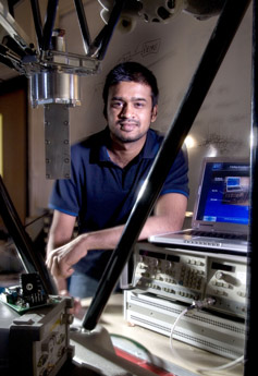
The research carried out by Prof Marc Desmulliez
at the James Watt Institute for High Value Manufacturing
led to the manufacture a proof-of-concept device
for variable frequency microwave heating and curing
of Micro electro Mechanical devices (MEMS). The
design of this device permits its easy installation
on to existing packaging technology for high accuracy
alignment capability.
The project has demonstrated that a set of process
conditions can be achieved so that variable frequency
microwave heating and cure technology can be implemented
successfully into electronic component manufacture,
assembly and packaging. New science-based engineering
has also emerged to understand the cure kinetics
of pastes used in MEMS packaging, which is radically
different from the curing achieved by heat convection
as the heat rate is orders of magnitude larger at
microwave frequencies.
This project enabled the creation of a unique, patentable
RF-cure apparatus for insertion into novel bonding
equipment that will permit a more efficient packaging
technology. A series of electronics industry associations
across Europe have identified the applications of
the technology and are to push the commercialisation
of the device to their members in November 2010
For more information contact:
Marc Desmulliez
m.desmulliez@hw.ac.uk
01314513340
misec.eps.hw.ac.uk
|